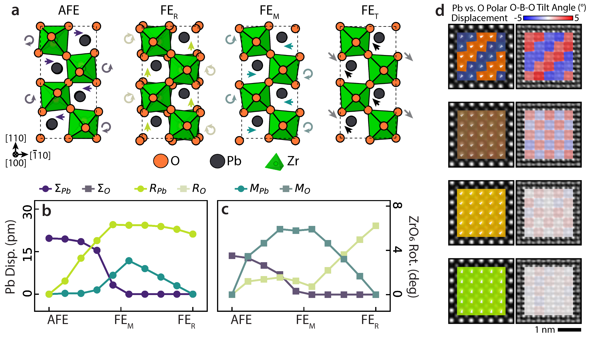
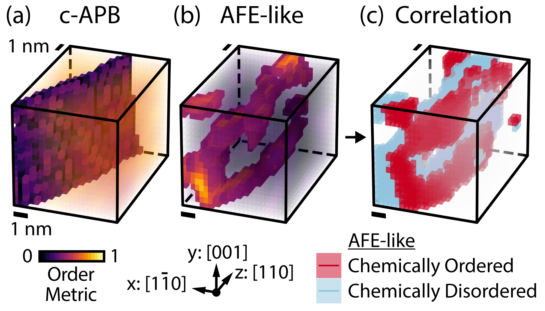
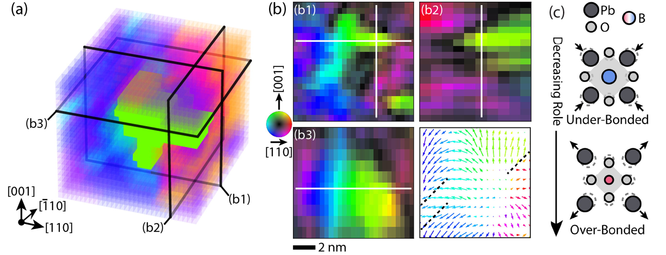
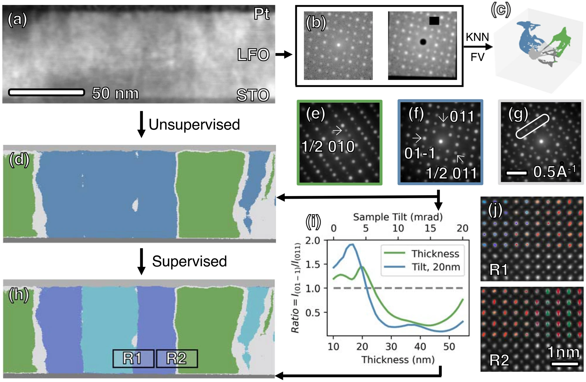
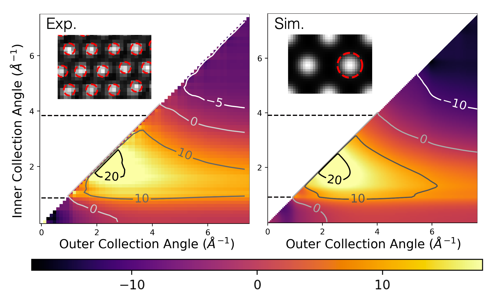
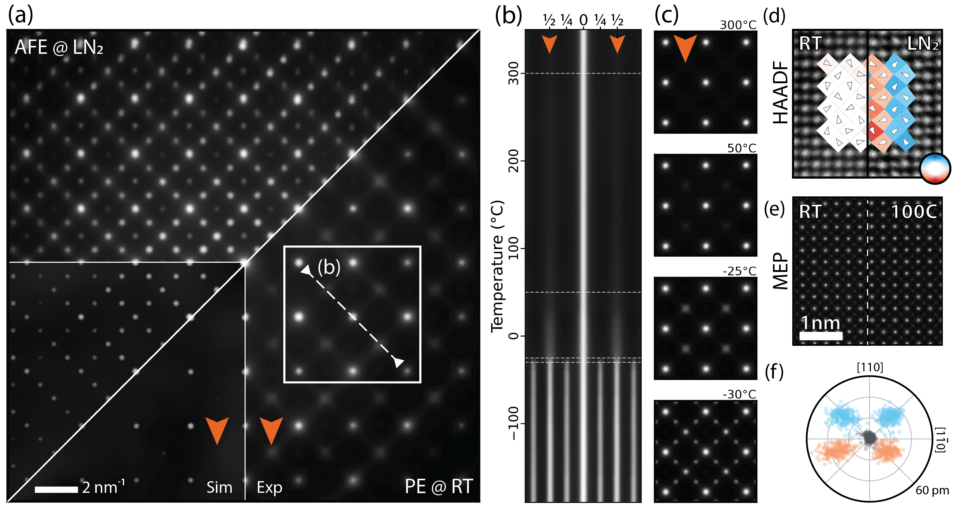
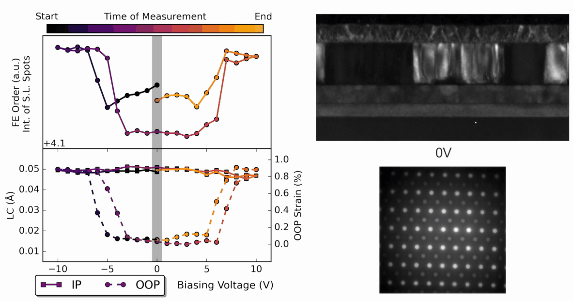
Projects

Preserving Device Geometry for Operando S/TEM Biasing

Preserving Device Geometry for Operando S/TEM Biasing

A lithography-based sample preparation strategy enables operando S/TEM biasing of thin-film devices while preserving as-grown architecture. Selective etching exposes the bottom electrode, and an insulating buffer barrier maintains electrical isolation. This approach retains original geometry, interfacial chemistry, and epitaxial strain states without relying on conductive substrates or artificially thick electrodes. Focused ion beam milling targets the buffer layer, minimizing damage and preserving device-relevant structure. The resulting configuration supports out-of-plane biasing under realistic conditions, allowing direct correlation between atomic-scale dynamics and bulk functionality. (Click to Read More)

Polar Slush of Relaxor Ferroelectrics in 3D

Polar Slush of Relaxor Ferroelectrics in 3D

Disruption of long-range order through heterogeneity can drastically alter material behavior, as seen in lead-based relaxor ferroelectrics. Decades of research have linked local chemical and structural inhomogeneities to unique macroscopic properties like high electromechanical coupling and broad dielectric response. While it is generally accepted that these inhomogeneities promote the relaxor response, various interpretations have emerged, ranging from the early model of polar nanoregions to the more recent polar nanodomain slush model. Here, we directly oberve the ploar slush in 3D using mutlislice electron ptychograpy. (Click to Read More)

Operando Obervation of AFE-to-FE Transtion

Operando Obervation of AFE-to-FE Transtion

Operando electron microscopy reveals the field-induced antiferroelectric-to-ferroelectric phase transition in thin-film PbZrO₃, marked by oxygen octahedra detilting and lattice-volume expansion. This transition, influenced by substrate constraints, results in enhanced electromechanical strain (1.7%) in 100 nm thick films. The atomic-scale pathway, including an intermediate transient phase, is also revealed. First-principles calculations support the mechanism, offering insights into thickness scaling for high-performance micro-/nano-electromechanical systems. (Click to Read More)

3D View of APBs and Spatially Corrleated AFE Nanodomains

3D View of APBs and Spatially Corrleated AFE Nanodomains

Multislice electron ptychography is used to characterize a chemical antiphase boundary in the double perovskite Pb₂MgWO₆, revealing its inclined orientation and finite chemical intermixing. 3D imaging shows antiferroelectric-like displacements near the boundary, contrasting with the paraelectric bulk. Spatial statistics and DFT calculations suggest these boundaries form due to kinetic constraints, with local chemistry influencing polar distortions. This study highlights the interplay between chemistry and polarization at APBs, offering insights for ferroic thin films. (Click to Read More)

Emergent Interfacial Magnetic States

Emergent Interfacial Magnetic States

Atomic resolution imaging combined with monochromated EELS reveals interfacial-mediated ferromagnetism driven by spin disproportionation in LaFeO₃/SrTiO₃. Epitaxial strain induces a checkerboard arrangement of low- and high-spin Fe<sup>3+</sup> ions at the interface, leading to ferromagnetism via superexchange interactions, offering insights for designing spintronic materials. (Click to Read More)

Machine Learning Assisted Phase Mapping from 4D-STEM

Machine Learning Assisted Phase Mapping from 4D-STEM

High-resolution characterization of domain structures across large scales is essential for unlocking the potential of domains and domain walls. 4D-STEM facilitates the collection of rich, spatially resolved diffraction data, yet traditional analysis methods often demand extensive prior structural knowledge. Integrating 4D-STEM with machine learning—both supervised and unsupervised—provides a powerful, scalable approach to analyze massive datasets and uncover hidden patterns without relying on preconceived models, opening new avenues for advanced material design and functional optimization. (Click to Read More)

Atomic Scale Debye Waller Thermometry

Atomic Scale Debye Waller Thermometry

Nanoscale temperature measurements are crucial for understanding the local thermal properties. As atoms vibrate more intensely with increasing temperature due to the larger Debye-Waller factor, the electron scattering cross sections are affected, leading to changes in the contrast of STEM images. This temperature sensitivity, experimentally demonstrated using 4D-STEM as a function of scattering angle, align well with multislice simulations, offering a promising method for atomic-scale temperature measurements. (Click to Read More)